|
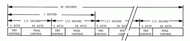
THEORY OF OPERATION 4-1 THEORY OF OPERATION MODEL 468-DC4-2 The 468-DC receiver decodes and outputs the time, using the NBS supported time code transmitted via the "GOES" (Geostationary Operational Environmental Satellite) Satellites, which are operated by NOAA (National Oceanic and Atmospheric Administration). 4-3 The transmission which carries the time code is at a frequency near 468 MHz. The data is encoded by phase shift modulation of the carrier (Manchester encoding) at a 100 bit per second rate. The code format breaks each second down into two ½ second sections, each consisting of 50 bits (½ of the available 100 bits in the second). During this ½ second, the first 4 bits * are used by the National Bureau of Standards for their controlled information.
4-4 The NBS Information consists of:
This information obviously cannot be conveyed in a single 4 bit character of a ½ second, therefore, one character each ½ second for 30 seconds is utilized. The data in items 1-5 above is repeated every 30 seconds. * The remaining 46 of the 50 available bits are used by NOAA for the purpose of "MAXIMUM LENGTH SEQUENCE" (MLS) which is a synchronization word and for data collection platform "Interrogation Address" which is the main purpose of their channel. 4-5 A phase locked receiver is used to receive and recover raw data from the satellite signal. The raw data is processed by analog circuitry and then passed to a microprocessor for conversion to useful outputs; among which are a visual display, one Hertz and one kilo Hertz timing pulses, and several optional communication ports. An overall block diagram of the hardware involved is given in FIGURE 4-2.
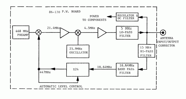
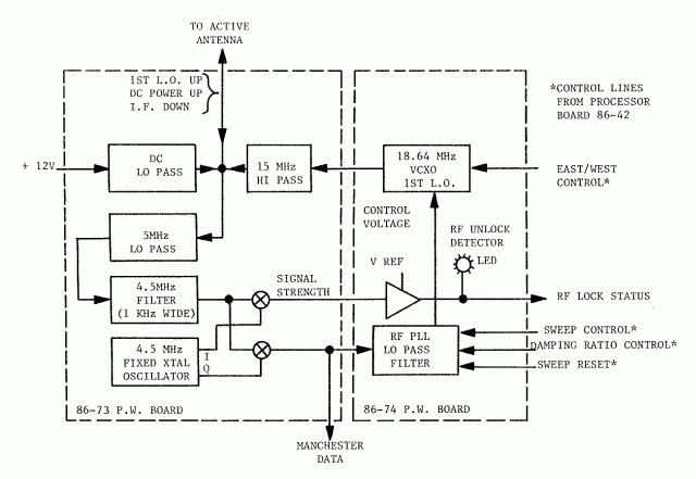
4-6 The receiver portion of the clock consists of the active antenna, the detector board (Assembly 86-73), and part of the analog board (Assembly 86-74) - all under control of the program on the digital board (Assembly 86-42). The active antenna receives the satellite signal, amplifies it by about 120 dB, and translates it in frequency to 4.5 MHz, using the first local oscillator frequency generated on the analog board in the main instrument and sent up the connecting coax together with the 12 VDC power. The second local oscillator is contained in the antenna. A block diagram of the active antenna is shown in FIGURE 4-3.
4-7 The 4.5 MHz output of the active antenna comes down the coax to the detector board (Assembly 86-73), where it is translated to baseband using the third local oscillator in conjunction with two balanced modulator/demodulators; one in phase, the other in quadrature with the satellite signal. 4-8 On the analog board, the in-phase baseband signal is an indication of signal strength, and is compared with a reference level to decide whether a satellite signal is being received. This information is passed on to the digital board, as well as being displayed by the LED RF unlock indicator. 4-9 The quadrature baseband signal constitutes the raw Manchester data and goes to the data phase locked loop. It is also used by the RF phase locked loop as the error signal to force the RF loop to stay in lock.
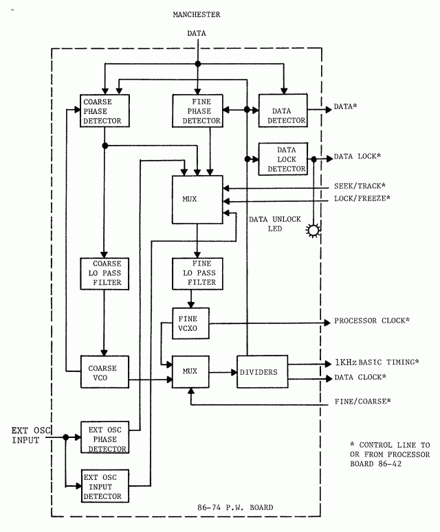
4-10 In order to recover Manchester coded data, two functions must be performed, synchronization (data clock recovering) and data decoding. The data PLL circuitry does both. There are two data PLL circuits, a coarse and a fine. The coarse PLL allows rapid sync to data at turn-on while the fine loop serves for precise sync once coarse sync is obtained. One or the other of these PLL's is always operating, under processor control. Whichever data PLL is selected runs the timing circuitry which supplies the timing for the processor and hence, all clock functions. Data clock recovery is performed by a PLL. At turn-on, a coarse PLL is used to quickly sync to the data. Thereafter, a fine PLL refines and maintains this sync. The fine PLL has three configurations, under processor control:
4-11 The data detector which decodes the raw Manchester data is an integrate and dump type, (which constitutes a matched filter for the code) and is located on the analog board. The output of the data detector goes to the processor for further analysis. 4-12 Also on the analog board is the external oscillator input, allowing use of a stable external oscillator during periods of interrupted signal reception; and the modulation circuitry for the IRIG-B time code output. 4-13 The microprocessor Board (Assembly 86-42) controls the whole instrument by means of the program stored in its memory. The program is discussed in the section on software, SECTION IV, entitled "SOFTWARE". All information in the instrument flows through this board. In addition to controlling the receiver's two phase lock loops and recovering the data, the 86-42 board provides all information for the front panel display, generates the several timing outputs of the clock, controls the timebase for the clock, and optionally communicates with the rest of the world via the RS-232, IEEE-488, or Parallel BCD interface. 4-14 The display board is controlled by the digital board. It contains multiplexed planar gas discharge displays and their drivers, providing an easily visible visual display of the time. 4-15 The output options also controlled by this board are the communications options. These boards (only one of which can be installed in an instrument) provide the ability to communicate the time to other instruments finding application in larger systems. Presently available options include Parallel BCD outputs, RS-232 Link, and IEEE-488 Bus capability. 4-16 DETAILED DESCRIPTION OF OPERATION4-17 ACTIVE ANTENNA ASSEMBLY 86-1704-18 The active antenna, A-468MS or A-468HX, contains a preamplifier, an IF amplifier and a first L.O. multiplier/mixer. See FIGURE 4-3 for a block diagram and SECTION VI for the schematic of Assembly 86-170. 4-19 PRE-AMPLIFIER4-20 Helical-tuned resonators provide 50 ohm matching as well as high selectivity at 468.8 MHz. Gain is greater than 8 dB and rejection at the image frequency, 426 MHz, exceeds 40 dB. TL1 and TL2 are quarter-wave stubs which are used to minimize out-of-band responses. 4-21 1st L.O. MULTIPLIER/MIXER4-22 The 18.64 MHz first L.O. signal from the main instrument is multiplied by 24 to provide the actual first local oscillator frequency. 468.8 MHz (signal frequency) - 21.4 MHz (first intermediate frequency) = 447.4 MHz (first local oscillator frequency). Automatic level control maintains the first L.O. power level at 0 dBm. 4-23 When the 18.64 MHz signal enters the board, it first passes through a high pass and a bandpass filter. Diodes CR4 and CR5 insure a constant drive level at Q3, which quadruples to 55.8 MHz in its collector circuit. Q4, 5 and 6 each act as doublers producing 447.4 MHz which is applied to the final drive stage, Q7. Helical filters, FL5 and FL4, serve to eliminate spurious signals which could cause undesired responses in the output of the mixer. Typically, undesired components are down by at least 60 dB. CR1 samples the 447 MHz level for the ALC circuitry. 4-24 Of the four sections of U1, one is the ALC amplifier, one drives the red 1st L.O. unlevel indicator LED; and the remaining two form a window comparator which lights the green "preamp active" indicator, if the preamp supply current demand is between 3 and 7 MA. 4-25 The balanced mixer takes the 447.4 MHz L.O. and the 468.8 MHz satellite signal and converts them to a signal at the 21.4 MHz IF. The output of the ALC amplifier, U1 pin 14, is applied as negative feedback to the emitter of Q5, thus closing the ALC loop. 4-26 INTERMEDIATE FREQUENCY AMPLIFIER4-27 The 21.4 MHz signal from the mixer passes first through Q2, acting as a buffer, and is then applied to a 13 kHz wide monolithic quartz crystal filter centered on 21.4 MHz (Y1 and Y2). This provides the primary protection against strong nearby signals, which can be common in the 468 MHz land mobile band. Q8 and Q9 and their associated components provide up to 40 dB of gain at 21.4 MHz. Y3 and Y4 are a second 21.4 MHz monolithic quartz filter which further reduce undesired signals, primarily internal receiver noise at this point. 4-28 Q10 is the second mixer. In conjunction with the 25.9 MHz second local oscillator, Q13 and Y5, the frequency is shifted down to 4.5 MHz, while providing 10 dB gain. Q11 and Q12 are the 4.5 MHz amplifier, which provide up to 60 dB gain. CR2 is the AGC rectifier. It samples the received signal, and by applying this sample to the AGC line, maintains a constant output level from the IF amplifier. 4-29 L25, C77, L26 match the high impedance 4.5 MHz output of the IF amplifier to 50 ohms for the transmission down line, and at the same time filter 18.6 MHz power to keep it out of the IF amplifier. 4-30 Power for the active antenna circuitry is provided by U2, an eight volt, three terminal voltage regulator. Nominal current consumption for the entire antenna is approximately 50 mA. 4-31 DETECTOR BOARD ASSEMBLY 86-734-32 Signals pass in both directions through the Detector Board. The 18.64 MHz first L.O. comes from the Analog Board Assembly 86-74, goes through the high pass filter C2, L4, C3 and then goes up the coax to the antenna. See Schematic SECTION VI for Assembly 86-73 and block diagram SECTION IV, FIGURE 4-4. 4-33 The 4.5 MHz signal from the antenna proceeds through the low pass filter L1, C4, L2 into the 4.5 MHz crystal filter T1, Y1, Y2, T2, R4 and then to the two balanced modulator/demodulators U2 and U3. The bandwidth of this filter is narrow, about 1 kHz. Q1, Q2 with Y3 are the third L.O., running at 18 MHz. U1 divides this by four to provide both in-phase and quadrature reference signals for U2 and U3. The frequency of the oscillator is trimmed by C9 to center the received signal in the 4.5 MHz filter passband. U2 and U3 phase detect the signal and output balanced baseband signals to the analog board. 4-34 ANALOG BOARD ASSEMBLY 86-744-35 See FIGURES 4-4 and 4-5 for a block diagram and SECTION VI for the schematic of Assembly 86-74. 4-36 RF LOCK DETECTOR4-37 The in-phase signal from U3 on the detector board is converted to a single-ended signal by U15 (pins 12, 13 and 14). It can be examined at TP2. Typically, this point is at -2.4V when locked to a satellite. Reliable decoding requires less than -1.0V. U15 (pins 1, 2, 3) is the signal strength comparator. The in-phase signal from U15 (pin 14) goes through a low pass filter to reduce the effects of modulation and noise, and is then compared with a reference level fixed at -0.6V. If the in-phase signal is more negative than the reference level, U15 (pin 14) extinguishes the RF unlock indicator (D7) and, through U25 (pins 7, 6) sends this information to the processor board. U25 serves merely as a level translator for signals going to the processor board from the analog board. 4-38 RF LOCK LOOP4-39 The Quadrature signal from U23 on the detector board is converted to single-ended by U15 (pins 8, 9, 10) and can be examined on TP3. This is the raw Manchester data from the satellite used by the data PLL's and the data detector. See FIGURE 4-6 below which depicts approximately 50 bits of superimposed data. 4-40 The Manchester data is then inverted and level-shifted compensate for offset voltage by U11 (pins 1, 2, 3) and by R45, the symmetry control. The signal then goes to the RF loop pass filter, U11 (pins 5, 6, 7). |